


Learning the printed circuit board terminology is key for clear communication. It’s vital when working with designers, engineers, and manufacturers. Knowing the basics of PCB manufacturing helps you make smart choices.
Knowing the PCB prototyping terms makes working with manufacturers smoother. It helps avoid mistakes and ensures your project is done right.
Grasping the main terms of printed circuit boards boosts teamwork. It makes sure your project succeeds.
Understanding PCB Basics
Learning about PCBs is key for making electronic devices. It helps you see how complex PCB prototyping is.
What is a PCB?
A Printed Circuit Board (PCB) is a board with conductive materials and components. It’s made of layers laminated together. Etched copper makes paths on each layer’s surface.
Types of PCBs
PCBs vary in type, including:
- Single-sided PCBs: These have conductive material on one side.
- Double-sided PCBs: These have conductive material on both sides.
- Multi-layer PCBs: These have multiple layers of conductive material, separated by insulating layers.
Each type is suited for different electronic devices, based on complexity and needs.
Common PCB Materials
The material choice affects a PCB’s performance and durability. Common materials are:
- FR4: A glass-reinforced epoxy laminate, used for its balance of cost and performance.
- Ceramic: Ideal for high-frequency applications because of its excellent dielectric properties.
- Metal Core: Needed for high thermal conductivity, like in LED lighting.
Choosing the right material depends on your project’s needs. This includes operating frequency, environmental conditions, and cost.
PCB Prototyping Fundamentals
Creating a prototype PCB is key to checking design ideas before making many copies. It’s important to know how PCB prototyping works. This helps in the design and making process.
Definition and Purpose
PCB prototyping means making a test PCB to check a design. Its main goal is to find and fix problems early. This saves time and money.
Key benefits of PCB prototyping include:
- Design validation
- Error detection and correction
- Performance testing
- Cost savings through reduced waste and rework
When to Create PCB Prototypes
You should make PCB prototypes early in product development or with big design changes. This ensures your design works and can be made.
Consider creating prototypes when:
- Testing new design concepts
- Making significant design changes
- Validating design simulations
- Preparing for mass production
Prototype Iterations
PCB prototyping means going through many versions of the design. You keep refining and testing until it’s just right. Each version gives feedback to make the design better.
| Iteration | Purpose | Outcome |
|---|---|---|
| 1st Iteration | Initial design test | Identify major design flaws |
| 2nd Iteration | Design refinement | Correct identified flaws |
| 3rd Iteration | Performance testing | Validate design performance |
Essential PCB Design Terminology
To work in PCB design, you must learn key terms. Knowing these helps you talk clearly with designers and engineers. This ensures your projects are done well and on time.
CAD Software Terms
CAD software lets you make a digital model of your PCB design. It’s important to know CAD terms for designing and changing PCBs. Some main terms are:
- Layer Management: This is about organizing different layers in a PCB design.
- Design Rule Check (DRC): It checks your design for mistakes and makes sure it follows manufacturing rules.
- Gerber Files: These are standard files that show the PCB layers for making it.
Schematic Capture Vocabulary
Schematic capture means drawing a diagram of electrical connections. Knowing schematic capture terms is key for making PCBs that work.
- Symbol: A picture of a component in a schematic diagram.
- Netlist: A list of connections between components in a schematic diagram.
- Hierarchy: This is about organizing complex designs into simpler parts.
Layout Design Language
Layout design language talks about the physical layout of the PCB. It’s important to know this language to make sure your design can be made and works well.
| Term | Description |
|---|---|
| Via | A hole drilled through the PCB to connect different layers. |
| Pad | A flat area of conductive material where a component is soldered. |
| Trace | A conductive path on the PCB that connects components. |
PCB Layer Terminology
When you start designing PCBs, it’s key to know the layer terms. The layer setup of a PCB is vital. It decides what your PCB can do and what it can’t.
Single-Sided vs. Double-Sided
PCBs are either single-sided or double-sided, based on their layers. Single-sided PCBs have just one layer. They’re simple and cheap for simple tasks. Double-sided PCBs have two layers. They let you make more complex designs and pack more into a smaller space.
Multi-Layer PCB Terms
If your design needs more than what double-sided PCBs offer, you go for multi-layer PCBs. These have three or more layers stacked together. Multi-layer PCBs help with complex designs, better signal quality, and less EMI.
- Multi-layer PCBs are for complex electronic devices.
- They improve signal quality.
- They cut down EMI.
Layer Stackup Concepts
The layer stackup is how the layers are arranged in a PCB. Getting the stackup right is key for good electrical performance. It helps control impedance and reduce EMI. The setup depends on the design, with different layers for signals, power, and ground.
| Layer Type | Description | Common Use |
|---|---|---|
| Signal Layer | Conductive layer for signal routing | Component connections |
| Power Plane | Layer dedicated to power supply | Power distribution |
| Ground Plane | Layer dedicated to ground connection | EMI reduction, signal reference |
Component and Connection Terms
To design a PCB, you must know component terminology. Components are the core of your PCB. It’s key to understand how they’re mounted and connected for a good prototype.
Through-Hole Technology (THT)
Through-Hole Technology mounts components through holes in the PCB. It offers strong connections and is best for components needing lots of power or specific mechanical needs.
Advantages of THT:
- Robust mechanical connections
- Suitable for high-power components
- Easier to prototype and repair
Surface Mount Technology (SMT)
Surface Mount Technology mounts components on the PCB’s surface. It’s great for small, dense designs and is perfect for high-density PCBs.
Advantages of SMT:
- Smaller component sizes
- Higher component density
- Improved electrical performance
Mixed Technology
Mixed Technology uses both Through-Hole and Surface Mount Technologies. It lets designers use THT for strong bonds and SMT for dense areas.
Benefits of Mixed Technology:
| Technology | Advantages | Applications |
|---|---|---|
| THT | Robust mechanical connections, suitable for high-power components | Power supplies, connectors |
| SMT | Smaller sizes, higher density, improved electrical performance | High-frequency circuits, compact designs |
| Mixed | Combines benefits of THT and SMT | Complex PCBs requiring both high power handling and high density |
Knowing component and connection terms is essential for PCB design. By picking the right technology or mix, you can make your PCB better, more reliable, and easier to make.
PCB Manufacturing Terminology
To understand PCB manufacturing, knowing the key terms is vital. It includes etching, plating, drilling, and routing. Each step has its own set of terms and jargon.
Etching and Plating Terms
Etching removes unwanted copper from the PCB. Chemical etching is the most common method. It uses a chemical solution to dissolve copper. Cupric chloride and ferric chloride are often used etchants.
Plating adds a layer of material to the PCB. Techniques include electroplating and electroless plating. Electroplating uses an electric current, while electroless plating uses a chemical reaction.
| Term | Description |
|---|---|
| Cupric Chloride | A chemical etchant used to remove copper from PCBs |
| Ferric Chloride | Another common etchant used in PCB etching |
| Electroplating | A plating technique that uses an electric current |
| Electroless Plating | A plating technique that uses a chemical reaction |
Drilling and Routing Vocabulary
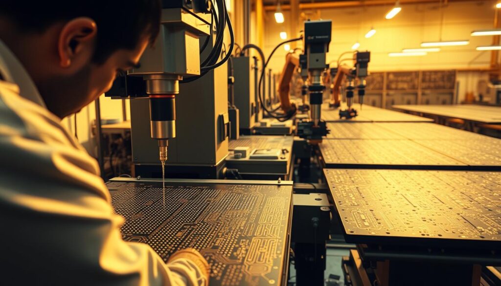
Drilling makes holes in the PCB for mounting components or vias. CNC drilling is a precise method.
Routing cuts out the PCB from a panel. A CNC router does this with precision, following the design.
Solder Mask and Silkscreen
The solder mask protects the PCB from unwanted solder flow. It’s applied by screen printing.
The silkscreen has text and symbols for component identification. It’s also applied by screen printing.
| Term | Description |
|---|---|
| Solder Mask | A protective layer to prevent solder flow onto unwanted areas |
| Silkscreen | A layer containing text and symbols for component identification |
| CNC Drilling | A precision drilling technique using computer numerical control |
| CNC Router | A machine used for cutting out PCBs from a larger panel |
PCB Prototyping Equipment and Tools
Understanding the tools used in PCB prototyping is key. You’ll see many machines and tools that help you make prototypes. These tools make creating prototypes efficient and effective.
CNC Machines
CNC machines are essential in PCB prototyping. They drill and route PCBs with great precision. You can program them to do tasks like making holes for components or cutting out the board.
Key Features of CNC Machines:
- High precision drilling and routing
- Programmable for specific tasks
- Ability to work with various materials
Laser Prototyping
Laser prototyping machines are another tool for precise PCB work. They use a laser to cut out and make holes. This method is great for complex designs and accurate results.
Advantages of Laser Prototyping:
- High precision and accuracy
- Ability to create complex geometries
- Minimal material waste
Chemical Etching Equipment
Chemical etching equipment etches PCBs using chemicals. It applies a resist, exposes it to a pattern, and then etches away unwanted copper. This method produces high-quality PCB traces.
Key Aspects of Chemical Etching:
- Application of resist to protect desired areas
- Exposure to the desired pattern
- Etching away unwanted copper
| Equipment | Primary Use | Key Benefits |
|---|---|---|
| CNC Machines | Drilling and routing PCBs | High precision, programmable |
| Laser Prototyping Machines | Creating precise cutouts and holes | High accuracy, complex geometries |
| Chemical Etching Equipment | Etching PCBs using chemical processes | High-quality traces, precise pattern transfer |
PCB Testing and Validation Terms
You need to know PCB testing terms to make sure your printed circuit board works right. PCB testing checks the quality and reliability of the board through different processes.
Electrical Testing Vocabulary
Electrical testing is key to checking your PCB’s integrity. It looks for continuity, shorts, and opens in the circuit. You should know about:
- Continuity test: Makes sure there’s a full path for the electrical signal.
- Insulation resistance test: Measures the resistance between conductors.
- High-potential (Hi-Pot) test: Sees if the insulation can handle high voltage.
Functional Testing Terms
Functional testing checks if your PCB works as it should. It tests the board under different conditions to mimic real-world use. Important terms include:
- Functional test: Checks if the PCB works as expected under normal conditions.
- Boundary scan test: Uses a test access port to check connections between integrated circuits.
- In-circuit test (ICT): Tests the PCB while it’s on, looking for faults in components and connections.
Quality Assurance Language
Quality assurance in PCB making includes steps to ensure the product meets standards. You should know about:
- Quality control (QC): Checks PCBs against set specifications.
- Certification: Meets industry standards like IPC or ISO.
- Audit: Examines the PCB making process to ensure standards are followed.
Knowing these terms helps you understand PCB testing and validation. This ensures your product is reliable and works as it should.
Common PCB Defects and Troubleshooting Terms
Understanding and fixing common PCB defects can make your electronic devices more reliable. These defects can come from how PCBs are made or from design choices.
Manufacturing Defects
Manufacturing defects happen when making PCBs. They include:
- Incorrect drilling or routing
- Insufficient or excessive solder
- Poor plating quality
Knowing about these defects is key for quality control. Fixing manufacturing defects quickly can prevent big losses and save money.
Design Flaws
Design flaws are problems in the PCB design that can cause issues. Common ones are:
- Inadequate clearance between components
- Incorrect component placement
- Insufficient via sizing
Design flaws can be fixed with careful design rule checking (DRC) and simulation. Finding problems early can save a lot of time and money.
Diagnostic Terminology
Diagnostic terminology is the language and methods for finding and fixing PCB defects. Important terms include:
| Term | Description |
|---|---|
| Short circuit | An unintended connection between two or more conductors. |
| Open circuit | A break in a conductor, preventing current flow. |
| Solder bridge | Excess solder connecting two or more pins. |
Knowing these terms helps designers, manufacturers, and test engineers talk clearly. 
Advanced PCB Prototyping Techniques
Advanced PCB prototyping uses special materials and processes. It creates complex, high-performance printed circuit boards. Techniques include rigid-flex PCBs, high-frequency PCBs, and embedded components.
Rigid-Flex PCBs
Rigid-flex PCBs mix rigid and flexible PCBs’ benefits. They offer better reliability and lower assembly costs. They’re great for tight spaces and mechanical stress.
- Aerospace
- Medical devices
- Military equipment
High-Frequency PCBs
High-frequency PCBs work at speeds over 1 GHz. They need special materials to keep signals strong.
| Material | Dielectric Constant | Applications |
|---|---|---|
| PTFE | 2.1 | High-frequency antennas, radar systems |
| RO4003 | 3.38 | Telecom infrastructure, high-speed data links |
| RO3003 | 3.0 | Aerospace, defense, high-frequency circuits |
Embedded Components
Embedded components are built into the PCB. This method boosts performance, cuts size, and raises reliability.
- Improved electrical performance
- Reduced PCB size
- Increased reliability
Navigating the Future of PCB Technology
The future of PCB technology is changing fast. New trends and innovations are leading the way. It’s important to keep up with these changes.
The PCB industry is always growing. New technologies and methods are making PCBs more complex and advanced. By knowing about these trends, you can use the latest PCB tech.
Key trends include better materials, new manufacturing ways, and design improvements. These changes will make PCBs work better, last longer, and do more.
To stay ahead, keep up with the latest in PCB tech and trends.
FAQ
What is a PCB?
A PCB, or Printed Circuit Board, is a board with conductive materials and components. They work together to produce a designed response.
What are the different types of PCBs?
PCBs come in various types. These include single-sided, double-sided, and multi-layer boards. Each type has its own characteristics and uses.
What is PCB prototyping?
PCB prototyping is about creating a prototype PCB. It’s used to test and validate a design. This helps identify and fix issues before mass production.
What is the purpose of CAD software in PCB design?
CAD software helps create a computerized prototype of a design. It lets designers visualize and refine their designs before manufacturing.
What is the difference between through-hole and surface mount technology?
Through-hole technology mounts components through holes in the PCB. Surface mount technology mounts components directly to the PCB’s surface.
What is etching in PCB manufacturing?
Etching removes unwanted copper from the PCB. It creates the desired circuit pattern.
What is the purpose of solder mask and silkscreen?
Solder mask and silkscreen protect the PCB and provide identification. They make it easier to assemble and troubleshoot the board.
What is electrical testing in PCB validation?
Electrical testing checks the PCB’s electrical integrity. It ensures the board functions as intended.
What are common PCB defects?
Common PCB defects include manufacturing errors like incorrect drilling or routing. Design flaws, such as inadequate clearance or incorrect component placement, are also common.
What are rigid-flex PCBs?
Rigid-flex PCBs combine the benefits of rigid and flexible PCBs. They enable the creation of complex and compact designs.
What is the significance of layer stackup in PCB design?
Layer stackup is the arrangement of conductive and insulating layers in a PCB. It’s critical for ensuring the board’s electrical performance and reliability.
What is diagnostic terminology in PCB troubleshooting?
Diagnostic terminology is the language used to describe the processes and procedures for identifying and fixing PCB defects. It enables efficient troubleshooting and repair.