


Did you know that bad PCB design can cause big delays and extra costs? Making your PCB design and prototyping process better is key. It helps you work more efficiently and get your projects done faster.
Learning the basics and best ways of PCB prototyping is important. It makes sure you go smoothly from design to production. Getting help from experts can make your electronic device development easier. This way, you can make products that work well and are reliable.
Using expert advice can make your PCB design and development better. This improves your workflow.
Understanding PCB Design Basics
Learning the basics of PCB design is key to making top-notch electronic products. You must understand the fundamentals to ensure your printed circuit board (PCB) works right.
What is PCB Design?
PCB design is about making the layout for a printed circuit board. It’s the core of most electronic devices. You’ll plan the circuit, pick components, and check if the design fits the specs.
The steps include making a circuit diagram and laying out components on the board. This is called schematic capture and PCB layout.
Importance of PCB Prototyping
PCB prototyping is a vital step. It lets you test your design, spot problems, and tweak it before mass production.
Prototyping confirms your design works as planned. It ensures it meets performance standards.
Here are some key benefits of PCB prototyping:
- Reduced Costs: Finding and fixing problems early saves a lot of money.
- Improved Performance: Prototyping lets you test and improve your design, leading to better results.
- Faster Time-to-Market: Validating your design through prototyping means you can launch your product sooner.
The following table summarizes the key aspects of PCB design and prototyping:
| Aspect | Description | Importance |
|---|---|---|
| PCB Design | Creating the layout for a printed circuit board | Essential for ensuring the PCB functions as intended |
| Prototyping | Testing the design to identify and fix issues | Critical for validating the design and improving performance |
| Components Selection | Choosing the right components for the PCB | Vital for ensuring compatibility and performance |
Key Steps in the PCB Design Process
Creating a PCB involves several steps that need careful planning and execution. You must follow a structured process to make sure your PCB works well and can be made.
Planning Your Design
The first step is planning your design. You need to define what your PCB should do, how it should perform, and its physical limits. Think about what components you’ll use, how much power it needs, and how signals will flow. Proper planning is key to avoid expensive changes later.
Schematic Creation
With a plan in place, you can start making a schematic diagram. This is done using special software to show how components are connected. The schematic is like a blueprint, making sure everything is connected right. Being accurate here is very important for your PCB’s success.
Layout Design
After the schematic, you work on the layout design. This is where you arrange components on the PCB and connect them. You must think about signal quality, heat management, and how easy it is to make. Good layout design makes your PCB work well and is easy to produce.
Design Rule Check (DRC)
The last step before prototyping is the Design Rule Check (DRC). This checks your design against rules to find any problems, like too little space or wrong trace sizes. A good DRC is vital to find errors early, saving you from costly fixes later.
By following these steps, you can make sure your custom PCB design is reliable and efficient. Whether you’re prototyping or making a final product, a well-designed PCB is essential for success.
Tools for PCB Design
The right PCB design tools can greatly improve your design process. You have many software options, each with its own features and benefits.
Popular PCB Design Software
Many software tools are used for PCB design. Altium Designer, Eagle, and KiCAD are some of the most popular. They offer features like schematic capture, SPICE simulation, and board layout.
| Software | Key Features | User Base |
|---|---|---|
| Altium Designer | Schematic capture, SPICE simulation, board layout | Professional engineers |
| Eagle | User-friendly interface, library support | Hobbyists, professionals |
| KiCAD | Open-source, cross-platform compatibility | Open-source community, hobbyists |
When picking a PCB design tool, think about your project’s needs. Consider ease of use, features, and how well it fits your workflow.
Online vs. Offline Tools
PCB design tools come in both online and offline versions. Offline tools like Altium Designer and Eagle have advanced features. Online tools are great for easy access and teamwork.
Offline Tools: They are best for complex designs and are often used by professionals.
Online Tools: They are easy to use from anywhere and help with teamwork.
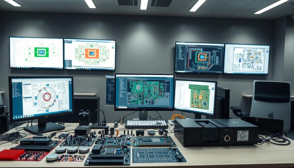
Choosing between online and offline tools depends on your needs. Consider your design’s complexity, teamwork needs, and personal preference.
Importance of Prototyping in PCB Development
Prototyping is key in PCB development. It makes sure your final product works well and is efficient. By making a prototype, you can test your design, find problems, and fix them before making many copies.
Prototyping offers several benefits that can greatly help your PCB project. Let’s look at these benefits more closely.
Benefits of Prototyping
One big plus of prototyping is finding design mistakes early. This lets you fix them before you make a lot of products.
- Reduced Costs: Finding and fixing problems early saves money and reduces waste.
- Improved Performance: Prototyping helps you test and improve your design. This makes sure your product works as it should.
- Enhanced Reliability: Testing and validating your PCB through prototyping makes it reliable and works as planned.
Common Prototyping Techniques
There are many ways to prototype PCBs, each with its own benefits. Some common methods are:
- Manual Prototyping: This is when you make a PCB by hand, like etching or milling. It’s good for small prototypes because it’s cheap.
- 3D Printing: 3D printing makes complex PCB designs quickly and accurately.
- CNC Milling: CNC milling uses machines to cut PCBs from raw material. It’s very precise.
Knowing about prototyping’s benefits and methods helps you make better choices for your PCB project. This ensures your project is a success.
Selecting the Right Materials
Choosing the right materials for your PCB is key for its performance and reliability. The materials used impact the PCB’s durability, thermal stability, and electrical properties. This makes material selection a critical step in low volume pcb prototyping and pcb design and prototyping.
Types of PCB Materials
There are many types of materials used in PCB manufacturing, each with unique characteristics. Common materials include:
- FR4: A glass-reinforced epoxy laminate, widely used due to its cost-effectiveness and decent electrical properties.
- Polyimide: Known for its high thermal stability and flexibility, making it suitable for applications requiring durability.
- Metal-core substrates: Used in applications that require efficient heat dissipation, such as LED lighting and power supplies.
| Material | Dielectric Constant | Loss Tangent | Thermal Stability |
|---|---|---|---|
| FR4 | 4.3-4.5 | 0.02-0.03 | Moderate |
| Polyimide | 3.4-3.5 | 0.002-0.003 | High |
| Metal-core | Varies | Varies | High |
Factors to Consider When Choosing Materials
When selecting materials for your PCB, several factors need to be considered:
- Dielectric Constant: Affects the signal propagation speed and should be considered for high-frequency applications.
- Loss Tangent: Indicates the material’s electrical loss and is critical for high-frequency designs.
- Thermal Stability: Important for applications that are exposed to varying temperatures.
By carefully evaluating these factors and understanding the properties of different materials, you can make informed decisions for your pcb design and prototyping projects. This ensures they meet the required specifications and performance standards.
PCB Manufacturing: What to Expect
When you choose to make your printed circuit board (PCB), knowing the process is key. It takes several important steps from design to a working PCB.
The Manufacturing Process
The PCB making process has many parts, like making, putting together, and checking. Important steps in making include:
- Choosing and getting ready the materials
- Putting the circuit design on the board
- Etching to remove extra material
- Drilling holes for parts and vias
Then, the assembly starts, where parts are put on the board. This is done with Surface Mount Technology (SMT) or Through-Hole Technology (THT).
Quality Control in PCB Production
Manufacturers use strict quality checks to make sure your PCB works well. These steps are:
- Looking at the board to find any problems
- Testing the electrical parts to check if they work
- Testing in different conditions to see how it holds up
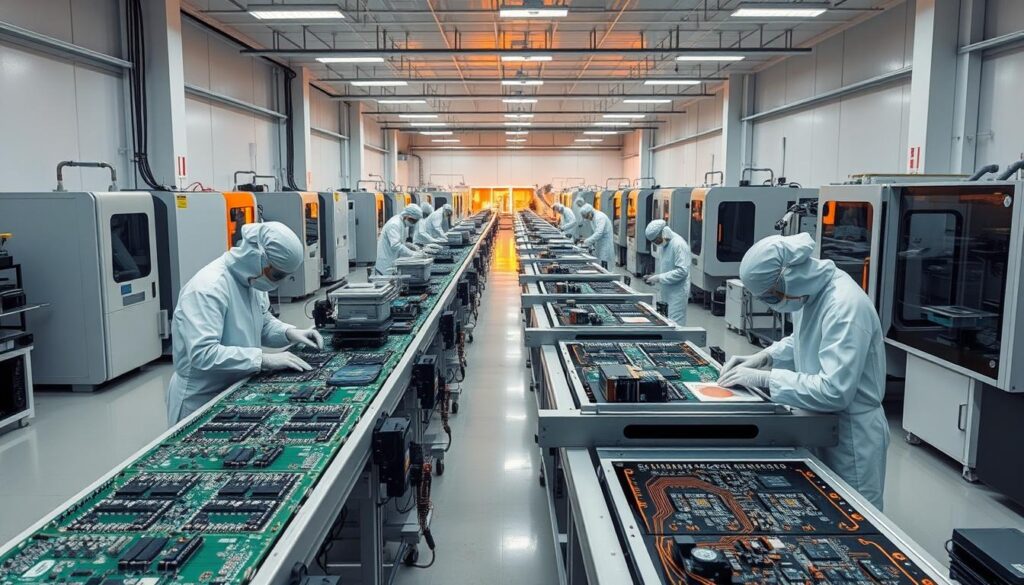
Knowing these steps helps you plan better. This way, your PCBs will be made to the best standards.
Testing and Validation of PCB Prototypes
Testing and validation are key to making sure your electronic prototype works as it should. This step is vital for finding and fixing any problems early. It saves time and money later on.
Why Testing is Crucial
Testing your PCB prototype is vital to check its performance and reliability. It lets you see if your custom PCB design works as planned under different conditions. This way, you can make sure it’s ready for mass production.
Reliability and Performance: Good testing boosts your PCB’s reliability and performance. It spots issues like signal problems, heat management, and how it works under various conditions.
Methods of Testing
There are several ways to test and validate PCB prototypes. These include:
- Functionality Testing: Checks if the PCB does what it’s supposed to do, performing all needed functions.
- Signal Integrity Analysis: Makes sure signals sent through the PCB aren’t affected by noise or distortion.
- Thermal Analysis: Examines the PCB’s heat management, ensuring it stays within the right temperature range.
Using these testing methods ensures your electronic prototype is strong, reliable, and market-ready.
Best Practices for Effective PCB Design
To make sure your PCB design works well and can be made, follow best practices. Good PCB design is key for your project’s success. It affects how well it works and how reliable it is.
Design Guidelines to Follow
When you design your PCB, there are important guidelines to follow. These help make sure your design is successful. They include:
- Proper component placement to minimize signal interference and optimize space.
- Careful trace routing to avoid signal degradation and ensure signal integrity.
- Design rule checking (DRC) to identify and correct issues before making it.
By following these guidelines, you can make your PCBs more reliable and perform better. For example, placing components right is key for rapid pcb prototyping. It affects how well your prototype works and how efficient it is.
Common Pitfalls to Avoid
Avoiding common mistakes in PCB design can save time and money. Some common pitfalls include:
- Insufficient clearance between components, which can cause manufacturing problems.
- Inadequate grounding, which can lead to signal noise and interference.
- Ignoring design for manufacturability (DFM) principles, which can raise production costs and delays.
Knowing about these common issues can help you design a better and more reliable PCB. For circuit board prototyping, it’s important to think about these factors. This ensures your prototype is both functional and ready for production.
Future Trends in PCB Design and Prototyping
You’re on the edge of a new era in PCB design and prototyping. This era is driven by new materials, automation, and AI. These changes will greatly affect your design process and how your products work.
Advancements in Materials and Technology
New materials and technologies are emerging in PCB design. They improve performance and efficiency. Expect better high-frequency materials, thermal management, and smaller designs.
These advancements will let you create more complex and advanced designs. You’ll use professional pcb design tools to do this.
Automation and AI in PCB Design
Automation and AI are changing the PCB design process. They make it faster and more efficient. AI tools can help optimize your design and predict problems.
For low volume pcb prototyping, automation speeds up testing and iteration. This means your products can hit the market faster.
By adopting these trends, you’ll stay ahead in PCB design and prototyping. The industry will keep evolving, and you’ll be ready to face new challenges. You’ll also be able to create innovative products.
FAQ
What is the importance of PCB design and prototyping in electronic device development?
PCB design and prototyping are key steps in making reliable electronic devices. They help find and fix design issues before mass production.
What are the key steps involved in the PCB design process?
The main steps are planning, creating a schematic, designing the layout, and doing a Design Rule Check (DRC). This ensures your PCB works well and can be made.
What tools are available for PCB design, and how do I choose the right one?
There are many PCB design software options. You can pick from online or offline tools. The right tool depends on your needs and affects your design’s quality.
Why is prototyping important in PCB development, and what are the benefits?
Prototyping helps find and fix design problems. It improves performance and ensures your product’s success. You can use various techniques to test your PCB design.
How do I select the right materials for my PCB, and what factors should I consider?
You have many PCB material options. Consider performance, reliability, and your specific needs when choosing.
What can I expect during the PCB manufacturing process, and what is the importance of quality control?
The process includes fabrication, assembly, and testing. Quality control is key to making sure your PCBs meet high standards.
Why is testing and validation critical in the PCB prototyping process?
Testing and validation are vital for your PCB’s reliability and performance. They help you find and fix issues early.
What are some best practices for effective PCB design that I should follow?
Follow design guidelines and avoid common mistakes. This improves your PCB’s reliability and performance, making it functional and easy to make.
What are the future trends in PCB design and prototyping that I should be aware of?
New PCB technologies, automation, and AI are changing the field. Staying updated with these advancements can help you improve your projects.
How can I optimize my workflow for PCB design and prototyping?
Learn the basics and best practices of PCB design. Use the right tools and follow a streamlined process. This will make your projects more efficient.
What is the role of rapid PCB prototyping in product development?
Rapid PCB prototyping lets you quickly test and validate your design. It saves time and money, helping you bring your product to market faster.
How does custom PCB design impact the performance of my electronic device?
Custom PCB design lets you tailor your PCB to your needs. It improves performance, reliability, and functionality.
What is low volume PCB prototyping, and when is it used?
Low volume PCB prototyping is for small production runs. It lets you test and validate your design before making more.
How does professional PCB design ensure the success of my project?
Professional PCB design focuses on manufacturability and performance. It reduces errors and improves reliability, ensuring your project’s success.
What is circuit board prototyping, and how does it differ from PCB prototyping?
Circuit board prototyping is creating a prototype of your PCB. It’s often used with PCB prototyping but includes more techniques and methods.
How can electronic prototyping services help me in my product development?
Electronic prototyping services offer expert guidance and support. They help you design, test, and validate your PCB, ensuring a smooth transition to production.